Ningbo Materials acquired series of organic/inorganic heterojunction solar cells
The current world record for the efficiency of silicon-based solar cell laboratories (25.6%) was created by Matsushita, Japan, and its device structure is based on the heterojunction form of crystalline silicon/amorphous silicon thin films (HIT cells). In the HIT cell, high-quality passivation of the monocrystalline silicon surface by the amorphous silicon thin film was fully utilized, and an extremely high open circuit voltage (740 mV) was obtained with extremely low interface electrical loss. With reference to the HIT structure, newly developed single-crystal silicon/organic heterojunction solar cells adopt a simple method of spin coating corresponding conductive organic materials on a silicon substrate and then depositing upper and lower metal electrodes to complete device preparation. The n-Si/PEDOT:PSS heterojunction constructed from n-type silicon and organic poly(styrenesulfonate) (PEDOT:PSS) with hole-conductivity type is excellent in this kind of battery. Representative, in which PEDOT:PSS can be modified to form a nearly perfect passivation effect on the silicon surface, with the potential to achieve high open circuit voltage (>700 mV) and high conversion efficiency (>20%). Ye Jichun, a researcher at the Institute of New Energy Technology under the Ningbo Institute of Materials Technology and Engineering, Chinese Academy of Sciences, combined his own advantages in the research and development of ultrathin monocrystalline silicon thin film materials, proposed the use of ultrathin monocrystalline silicon with a thickness of 20μm to build a new type of n-Si/ PEDOT: PSS heterojunction solar cell research direction and made a series of progress. Compared with conventional bulk silicon, the ultra-thin hybrid heterojunction cell not only has the characteristics of material saving and flexibility, but also reduces the effective transmission path of photocarriers and suppresses the body composition as the thickness is reduced. Theoretically, higher open circuit voltages can be obtained, and at the same time, the requirements on the quality of silicon materials can be reduced. The research team first designed a two-dimensional nanophotonic crystal suede to suppress the reflection of incident light on the front surface, and used the optical waveguide effect to grow the characteristic wavelength light on the silicon wafer. Internal transmission of the effective optical path. In order to solve the problem of array structure masking in the process of photonic crystal preparation, a novel method for preparing a two-dimensional periodic mask of a single molecular layer of polystyrene beads (PS) was independently developed. The method uses a multi-channel micropump injection system directly A PS monolayer self-assembled monolayer film was prepared on the liquid surface and then transferred to a pre-set silicon wafer. Based on this method, the team first demonstrated a large-area PS monolayer sample >1 m2 and designed a fully automatic micropunch injection prototype with a yield of >3000 tablets/h (matched to the photovoltaic industry). The PS ball mask technology has taken a big step towards industrialization. With the help of high-quality PS ball masks, combined with fully-scale mass production of wet etching (acid or alkaline corrosion) technology, the team succeeded in preparing nano-pillars and nanometers on a 20 μm-thick thin-film silicon substrate according to the design dimensions. Pyramids (or inverted pyramids), nano-pencils, and other characteristics of nano-photonic crystal suede structure, and access to the full band near the optical absorption of the trapping effect. The above related studies have applied for Chinese patents (201510084323.8, 201410196870.0, 201420239374.4, 201410196601.4, 201310480369.2), and the research results were published in the journal of Nano Letters (2015, 15, 4591). In the prepared array of textured structures, the nanopencil structure has a binary configuration with a nanocone at the top and a nanocolumn at the bottom, and the nanocones at the top have excellent structure change characteristics (impedance matching), which contributes to The direct reflection loss of incident light is minimized, while the lower nanocolumn structure helps to increase the scattering of incident light (increasing the effective optical path length). At a texturing depth of only 1.5 μm, the nanopencil structure helped the film silicon achieve excellent light trapping (average reflectance of less than 1.5% in the 400-900 nm band). At the same time, the tapered structure with a large open top facilitates the formation of a good coating of the conductive polymer PEDOT:PSS, increases the junction area of ​​the n-Si/PEDOT:PSS heterojunction cell, and enhances the carrier collection efficiency. . The new nano-textured structure responds to the problem that the nano-textured structure solar cell cannot achieve both optical and electrical gain at a certain level. The photoelectric conversion efficiency of the 20 μm-class hybrid solar cell prepared by optimizing the frontal structure alone exceeds 12%. . This method provides a new idea for the preparation of high-efficiency solar cells by suede morphology control, and the relevant results were accepted by Advanced Energy Materials (2015, DOI: 10.1002/aenm.201501793, In press) magazine. To further improve the photoelectric conversion efficiency of the n-Si/PEDOT:PSS heterojunction cell, the team focused on suppressing the carrier recombination at the back of the cell. By introducing a highly doped layer on the backside, a suitable back surface electric field is formed, which reduces the recombination of electron-holes on the surface by effectively reducing the concentration concentration of minority carriers on the surface. The highly doped layer also helps reduce the barrier to electron transport to the back-electrode while reducing the resistive contact loss with the back-electrode. As a result, the team fabricated an n-Si/PEDOT:PSS heterojunction solar cell with a photoelectric conversion efficiency of over 13.6% on a 20 μm thin film silicon substrate. This efficiency is comparable to the highest efficiency of the 300 μm bulk silicon hybrid batteries reported so far. The study provides a viable idea for the development of low-cost, high-efficiency thin-film heterojunction solar cell devices. Related results were published in the ACS Nano (2015, 9, 6522). At present, the research focus of the team on the direction of ultra-thin monocrystalline silicon hybrid heterojunction solar cells focuses on optimizing organic/inorganic interface contact and conquering device stability problems. The open-circuit voltage and conversion efficiency of the device are expected to reach the target in the near future. 680 mV, 15%, efficiency attenuation under long-term storage conditions (1 year) is controlled within 10%. The above work was supported by the National Natural Science Foundation of China (61404144, 21403262), Zhejiang Outstanding Youth Science Foundation (LR16F040002), Natural Science Foundation of Zhejiang Province (LY14F040005), Zhejiang Provincial Postdoctoral Scientific Research Project (BSH1402078), and Ningbo Natural Science Foundation (2014A610041). , 2013A610030) and other projects support. Measuring Tape MID certification; ISO9001 certification; 5M Measuring Tape,5M Tape Measure,Contractor Rubber Tape Measure,Heavy Use Measuring Tape Oukelong Tools Co.,Ltd , https://www.oukelongtape.com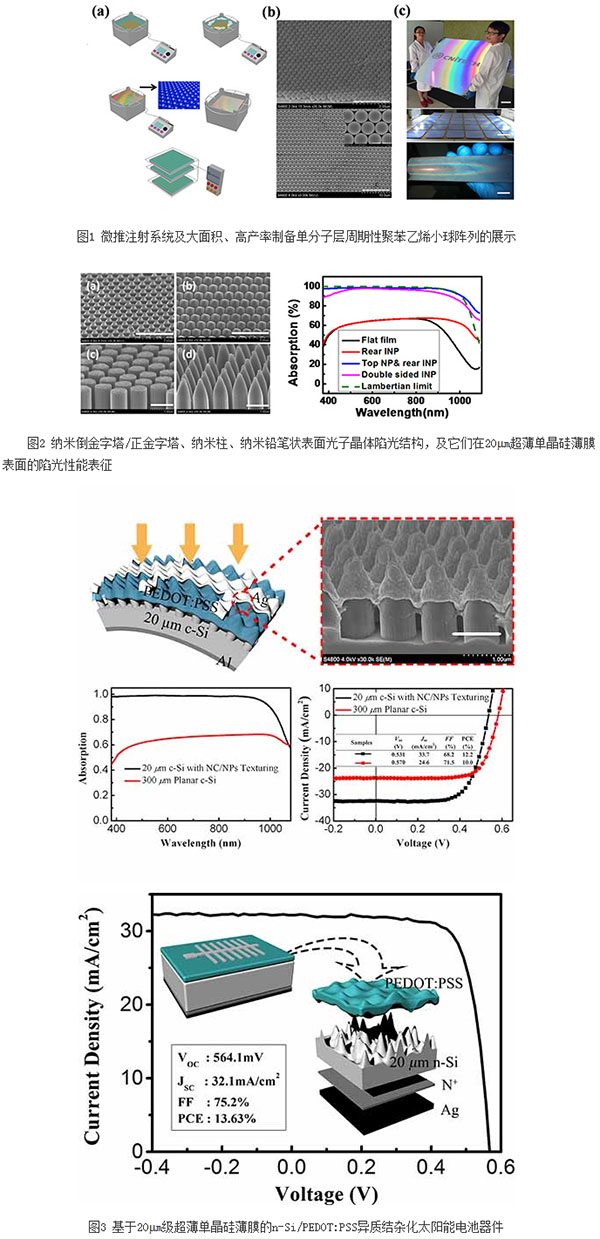
1. Measuring tape Case: First-grade new ABS plastics: Bright, odorless.
2. Graduation: British-metric; metric; British; Luban etc.
3.Measuring tape Blade: steel,white and yellow colors,matt and shiny or chromed
4. Hook: Magnetic or common (it depends on custom request) the hook is flexible
5. Rivets: 3or 2 rivets hook reduces risk of breakage; the rivet can be fastened to a proper position
6. Belt: The belt is made with Nylon for more handy and durable
7. Measuring tape Size: 1m/3ft-10m/33ft
Free Samples
We will offer you free sample within 5 working days after your comfirmation of details and invoice.
Quality Guarantee
We will check the products strictly one by one before arranging the shippment.
Price Discount
We will give discount to the long term business partners or the big order.
Customized Service
We can offer the OEM service based on clients' requirements such as the color,label or the package,etc.